Introduction
The firmware is the embedded software that controls the basic functioning of electronic devices, from routers and IP cameras to smart home appliances and industrial systems. Unlike traditional software, firmware operates directly on hardware, making it a critical target in terms of security, functionality, and privacy.
Firmware analysis involves examining this embedded software to understand its internal workings, detect potential vulnerabilities, identify backdoors, and in some cases modify or extract relevant information. This type of analysis is particularly relevant in security audits, forensic investigations, reverse engineering, or exploit development.
In this case, the firmware has been extracted from a device based on the Nordic nRF51 SoC, which uses the Cortex-M0 processor with ARM instructions, via SWD as described in this article. Not only was the firmware extracted but also the entire internal memory from hexadecimal address 0x0 to 0x40000, 262144 bytes, or 256 KB. For analysis purposes, we will use the disassembler and decompiler Ghidra.
Upon disassembling the file, we will obtain ARM assembly code instructions. Instructions referring to functions within the code itself can be found in the range 0x0-0x40000, but the embedded system may use other memory addresses for RAM or peripherals, which Ghidra is unaware of, so we will have to load them from a CMSIS-SVD file using the GhidraSVD plugin.
Loading Firmware into Ghidra
Before loading the firmware into Ghidra, we need to consider the initial address of the firmware, which can be extracted from its specifications in this case, in section 3.2 Memory.
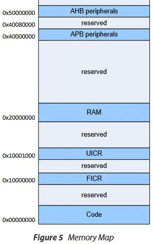 We observe that the code address is
 0x00000000, the FICR address is 0x10000000, the UICR address is 0x10001000, the RAM address is 0x20000000, and the peripheral addresses are 0x40000000 and 0x50000000. Each SoC has different memory addresses, and if they are not specified correctly in Ghidra, errors will occur during disassembly when searching for function references. For example, the start of STM32’s flash memory is hexadecimal address 0x08000000.
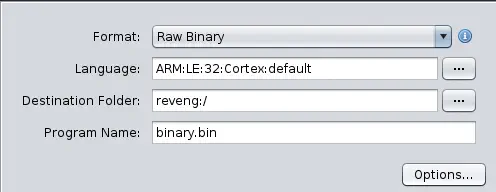
After opening Ghidra, we create a new project using File > New Project... as type Non-Shared Project, which will be saved in an existing folder beforehand. We then load the file from File > Import File... and select the binary file. A form appears where we need to specify its format (Format) as Raw Binary, its architecture (Language) as cortex (ARM Cortex / Thumb little-endian).
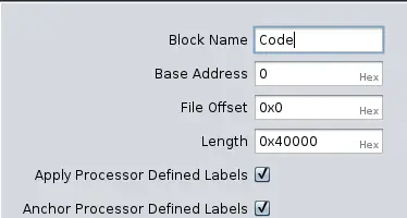
 Finally, in
 Options..., we can specify the starting address in memory (Base Address) if it differs from 0x0. In this case, we classify the name of the block (Block Name) as Code.
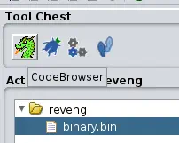
 The file will be loaded into the project list, and we can open it by selecting the file and dragging it to the
 CodeBrowser button (dragon icon).
Initial Analysis
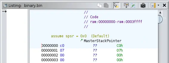
Upon opening the CodeBrowser, it informs us that the file has not been analyzed and asks if we want to analyze it. For now, we ignore it by pressing the No button. At this point, we already see the first hexadecimal bytes of the unanalyzed file.
 Before automatic analysis, we need to load memory addresses referring to different peripherals on the SoC to facilitate analysis. For example, if we find a code portion referencing a GPIO pin, we can observe the PCB and use a multimeter’s continuity option to search for where that pin is connected. It might be connected to a button or an LED diode, as examples. We also need to know the memory address of RAM to identify reads and writes in it.
The description of these addresses can be found in CMSIS-SVD files. A repository for them is available on Github. Ghidra cannot natively load these files, so we will use the GhidraSVD plugin.
Installing GhidraSVD Plugin
Firstly, we download the latest release of the plugin compatible with our Ghidra version. It is crucial that the plugin version matches the Ghidra version; otherwise, it will not work and return an exception.
$ wget https://github.com/antoniovazquezblanco/GhidraSVD/releases/download/v0.3.4/ghidra_11.3_PUBLIC_20250315_GhidraSVD.zip
The plugin is extracted into the GhidraSVD folder. We then go back to Ghidra and load the plugin by following these steps: open the extension manager using File > Install Extensions in Ghidra’s main window, press the Add extension button, which will open the Select Extension window, add the .zip file of the plugin we just downloaded to the list, and finally restart the program. We then reload the project with CodeBrowser. Now, an option to import the SVD file is available: File > Load SVD File....
Loading SVD File
We clone the repository containing the CMSIS-SVD files and search for the one corresponding to our SoC, in this case, cmsis-svd-data/data/Nordic/nrf51.svd. We load it with the option described above.
$ git clone --depth=1 https://github.com/cmsis-svd/cmsis-svd-data
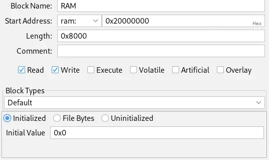
In some cases, the SVD file may not include the range of RAM memory. In this case, we will have to add it manually. By consulting the specifications, we find that the maximum size of RAM memory is 32 KB, 32768 bytes, or 0x8000 bytes. So, starting from address 0x20000000, its final address will be 0x20008000. To add the range of memory, we use the Window > Memory Map option and press the Add a new block to the memory option, specifying the data. Initially, it will only be an area for reading and writing, which does not contain code (Read and Write). We initialize the region with bytes 0x00.
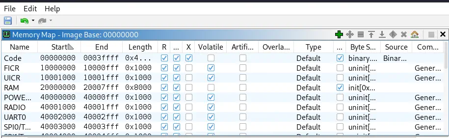
 We observe all memory regions.
Analysis
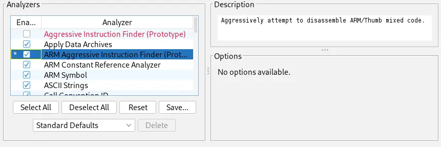
Now we can analyze the file using the Analysis > Auto Analyze option. The Analysis Options window will appear, where in this case, besides the default options, the Aggressively attempt to disassemble ARM/Thumb mixed code. option is enabled.
 After a few seconds, the code is disassembled and decompiled into pseudocode. For example, we find a function at memory address
 0x000028f2 with an auto-assigned name LAB_000028f2.
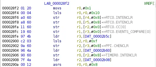 Thanks to loading the SVD file, we observe references to the device’s real-time counter (RTC) register,
 RTC0.INTENCLR. We will have to consult the manufacturer’s documentation to relate the register name with its meaning. For example, for the nRF51, we have a reference manual. In the case of more modern chips like the nRF52, we have more detailed explanations on their website documentation.
Conclusion
From now on, analysis will be based on reading the SoC’s reference manual to find different memory regions within the code. Not all will be user code; in several memory addresses, you will find libraries from the manufacturer that directly communicate with the device’s peripherals, for example, in this case, Bluetooth radio.